How Huawei's Tau Scaling Law Reinvents Telco Chip Design

The semiconductor industry has followed a simple formula for a long time.
It makes transistors smaller to fit more onto a chip, expecting performance to improve.
However, that model has now reached its limits as chipmakers face rising manufacturing complexity and shrinking returns from traditional scaling methods.
Huawei believes the next phase of computing depends less on shrinking components and more on moving data faster.
The company has introduced the Tau Scaling Law as a new approach to semiconductor design, one that focuses on reducing signal transmission time across chips and computing systems instead of reducing transistor size alone.
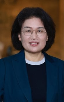
It was announced during a keynote speech by He Tingbo, Co-President of Huawei, at the 2026 IEEE International Symposium on Circuits and Systems in Shanghai.
Tingbo's peers and colleagues at Huawei named the principle Her’s Law.
Huawei moves chip design from 2D to 3D
At the heart of the Tau Scaling Law sits LogicFolding, Huawei’s methodology for redesigning chip architecture in three dimensions.
Traditional semiconductor design places components across a flat two-dimensional surface, creating longer distances for signals travelling between circuits.
Those transmission delays can become a bottleneck for telco systems handling large data volumes. Huawei argues that moving from horizontal layouts to vertically stacked structures reduces the distance information travels and improves speed and energy efficiency.
LogicFolding layers multiple two-dimensional planar circuits on top of one another, creating what Huawei compares to a multi-storey building instead of a single-storey structure.
The architecture places core circuits closer together and creates room for higher transistor density without relying entirely on smaller manufacturing processes.
The company states that shortening signal transmission time is critical because transmission time acts as a key indicator of processor frequency and overall performance.
By reducing resistive and capacitive load during signal propagation, the design increases computational speed while also improving energy use.
Four-level optimisation for telco systems
Huawei has said the Tau Scaling Law works through a multi-level co-optimisation mechanism that reduces the time constant τ across semiconductor devices, circuits, chips and systems.
At the device level, the company focuses on reducing resistance and parasitic capacitance in transistors and interconnects.
Parasitic capacitance refers to unwanted electrical charge storage that slows signal transmission. Lowering these effects reduces delays at the physical layer of semiconductor operation.
At the circuit level, LogicFolding shortens critical-path wiring. Critical paths represent the longest routes signals travel inside a circuit and often determine processing speed. Huawei said reducing these paths improves transistor density and circuit performance while lowering resistive and capacitive load.
At the chip level, Huawei applies coordinated design across software, architecture and silicon. The company said this creates workload-driven management of instruction and data flows, improving parallelism across computing systems.
Across computing systems, Huawei has introduced UnifiedBus, an interconnect protocol for computing systems.

Interconnect protocols govern how processors, memory and other hardware components communicate.
Huawei has said that UnifiedBus enables unified memory addressing and native memory semantics for SuperPoDs while reducing communications latency across systems.
Lower system latency supports applications such as AI-assisted radio access networks and real-time analytics.
Faster processing also benefits cloud-native telco services and distributed edge computing platforms.
Smartphone roadmap targets next-gen networks
Huawei already designs and mass-produces hundreds of chips using the Tau Scaling Law framework. During the keynote, Tingbo stated the company has developed 381 chips over the past six years using the principle for multiple industries and markets.
The first Kirin chips using LogicFolding architecture are scheduled for launch in autumn 2026. The processors will deliver higher performance for consumer devices including smartphones.
The company also outlined a longer-term semiconductor roadmap extending to 2031. Huawei is expecting its high-end chips based on the Tau Scaling Law to reach transistor density equivalent to 14 Å processes, representing a 1.4 nm scale.
Huawei positions the Tau Scaling Law as an alternative route for sustaining semiconductor performance gains, as conventional transistor scaling becomes harder to achieve.
Tingbo said: “We believe that openness and collaboration are key to driving ongoing progress in the semiconductor industry.
“No single company can independently find all the answers along the path of semiconductor evolution.”